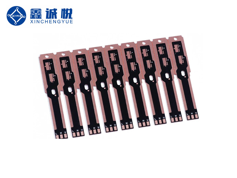
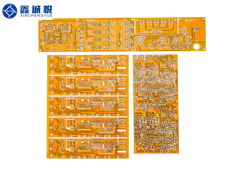
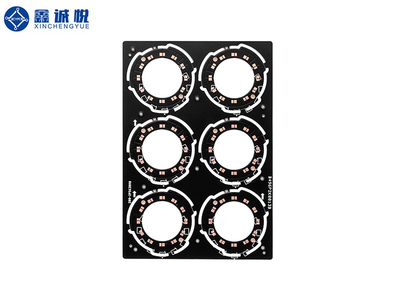
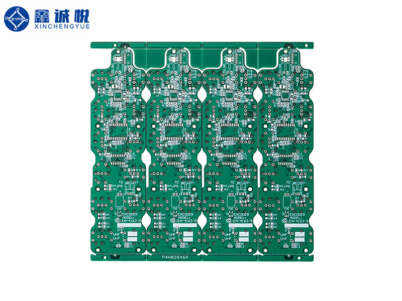
Single-sided copper substrate
1. Productivity: the use of modern management, standardization, scale, automation and other production, to ensure product quality consistency. 2. Can be high density: with the improvement of integrated circuit integration and installation technology progress and development. 3. Testability: Establish complete inspection methods, inspection standards, and various inspection equipment and instruments to test and identify the conformity and service life of PCB sample products. 4. High voltage resistance, high thermal conductivity, the performance of the metal substrate insulation layer directly affects the core performance of the metal substrate, the insulation layer uses nano-scale electronic thermal conductive adhesive film to make the product higher voltage resistance, faster heat dissipation, and increase the life of the end product. 5. The product complies with the EU environmental protection directive: PCB uses environmental protection materials in the whole process from raw material feeding inspection to finished product delivery, and regularly passes through the third-party inspection agency for inspection and control.
Classification:
Copper substrate
Product Consulting
Product Description
| Plate thickness | 2.0MM | Material | copper substrate | Number of layers | 1 | coefficient of thermal conductivity | 3.0W/M.K |
| Copper thickness | 70UM | Minimum line width | 0.6MM | Solder mask color | White | Surface treatment | OSP |
| Process characteristics | High thermal conductivity, thick copper | Fire rating | 94V0 | Environmental standards | ROHS | Application Scenarios | Lighting appliances |
| Minimum specifications | 100*80MM | Maximum size | 600*1200MM |
Previous Page
Next Page
Related Products
Product Message


